Ultraviolet lithography plays a critical role in the development of modern integrated circuits. Ultraviolet lithography is the process of transferring design pattern on wafers through spatially selective exposure of ultraviolet light onto the photoresist. Followed by the lift off and etching/deposition processes, micron sized structures can be achieved. The critical dimension and accuracy are the key parameters of the lithography machine, which directly determines the precision of the integrated circuit.
Conventional lithography systems require customized photomasks which are not only expensive but also time consuming to fabricate. Any changes in design patterns will require fabrication of new photomasks. Laser direct writing technology on the other hand can achieve decent critical dimension with excellent flexibility. Nevertheless, because of the point-by-point scanning across the whole wafer to transfer the pattern, the writing efficiency is relatively low. Recently, a new technology based on spatial light modulator (SLM) e.g. DMD/DLP has made great progress in ultraviolet photo lithography. Comparing to laser direct writing technology, SLM-based lithography has the added advantage of much higher efficiency while retaining the high precision and flexibility of laser writing.
TTT-07-UV Litho-Y table-top maskless UV lithography machine guarantees an outstanding critical dimension of 1.5 µm (objective lens A). The machine is equipped with high-performance direct drive linear motors with 50 nm closed-loop encoder system, and supports a wide range of wafer dimensions from 3 mm to 2-inch. The DMD-based lithography technology is equivalent to a programmable digital photomask possessing numerous advantages such as high efficiency, high flexibility, high resolution and high reliability. The equipment can be utilized in many studies, such as two-dimensional materials, electrical transport testing, photoelectric testing, terahertz and millimetre wave devices.
>>Key specifications (TTT-07-UV Litho-Y)

>>Application examples
>>Key Features
Desk-top lithography machin
Flexible pattern desig
Precise multi-step lithograph
Support up to 2-inch wafer
Minimum critical dimension 1.5 μm
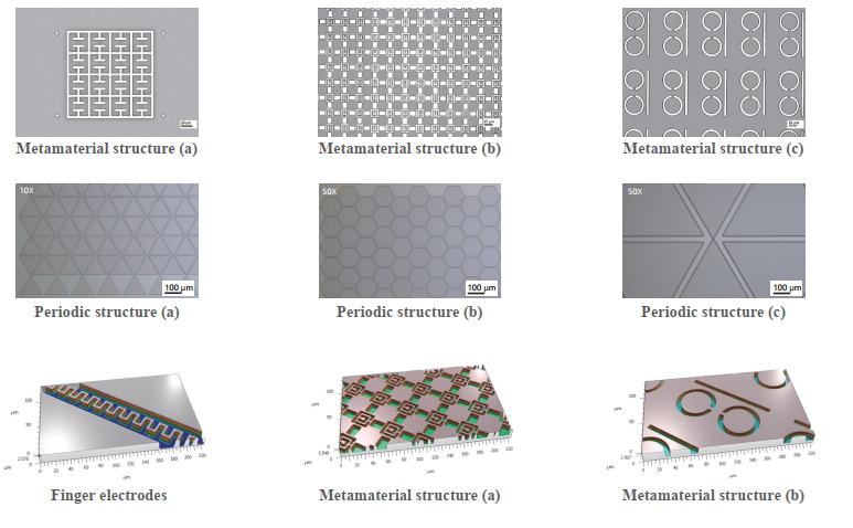
>>Application examples
Microfluidic chip
Micro / Nano structure exposure
Electrical transport test photoelectric test device
Electrode fabrication for 2D materials
Terahertz / millimetre wave device fabrication
Fabrication of optical mask
>>Upgradable options
1.Active vibration isolation
2.Glovebox enclosure
>>Installation requirement
· Temperature: 20–40℃
· Relative humidity: RH < 60%
· Power: 220 V, 50 Hz